
Item NO.:
GS-C025Payment:
L/C、 Western Union、 D/P、 T/TProduct Origin:
Anhui, ChinaMax Size:
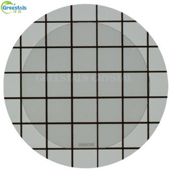
Dia100mmOrientation:
<100>、<110>、<111>Package:
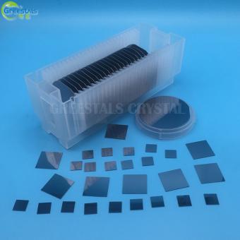
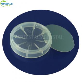
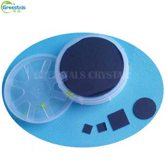
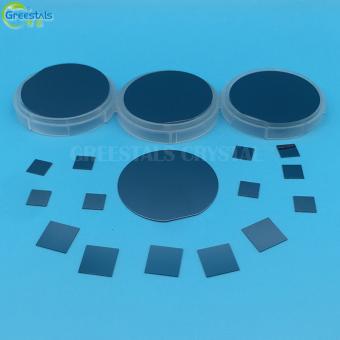
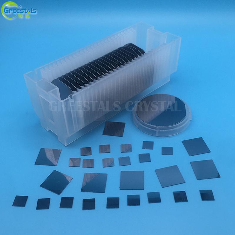
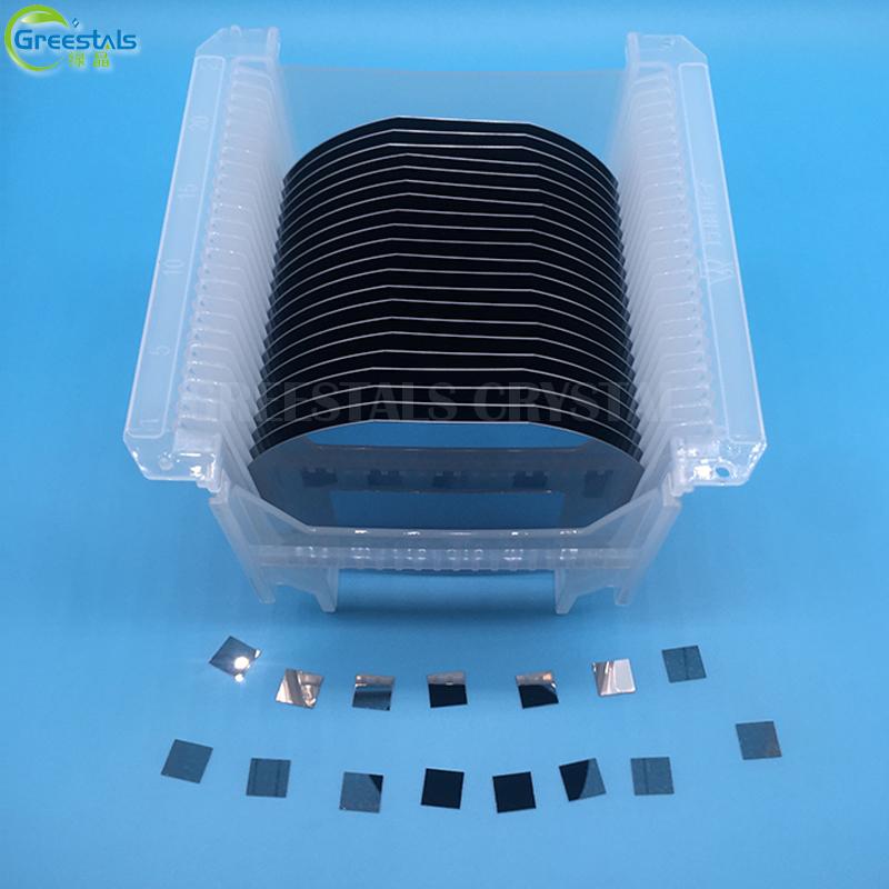
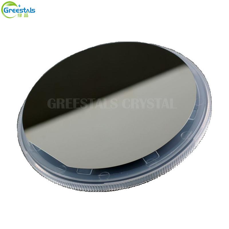
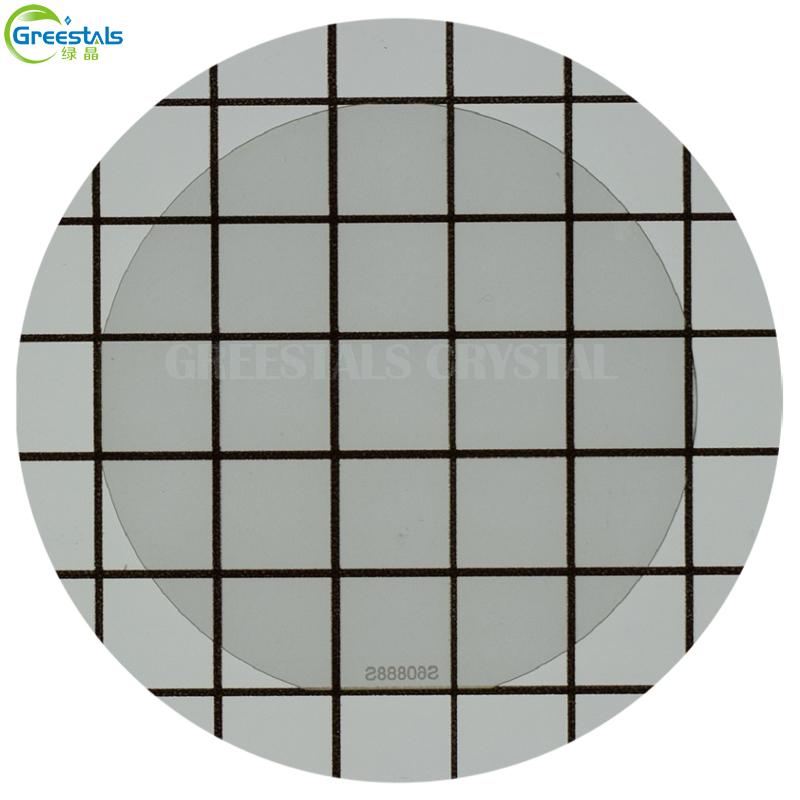
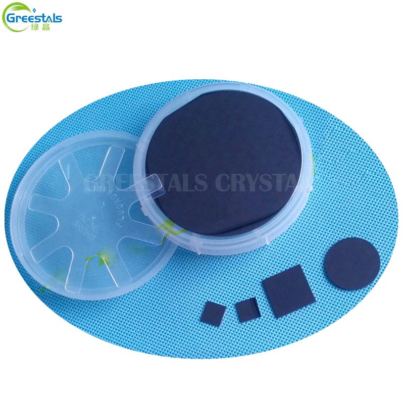
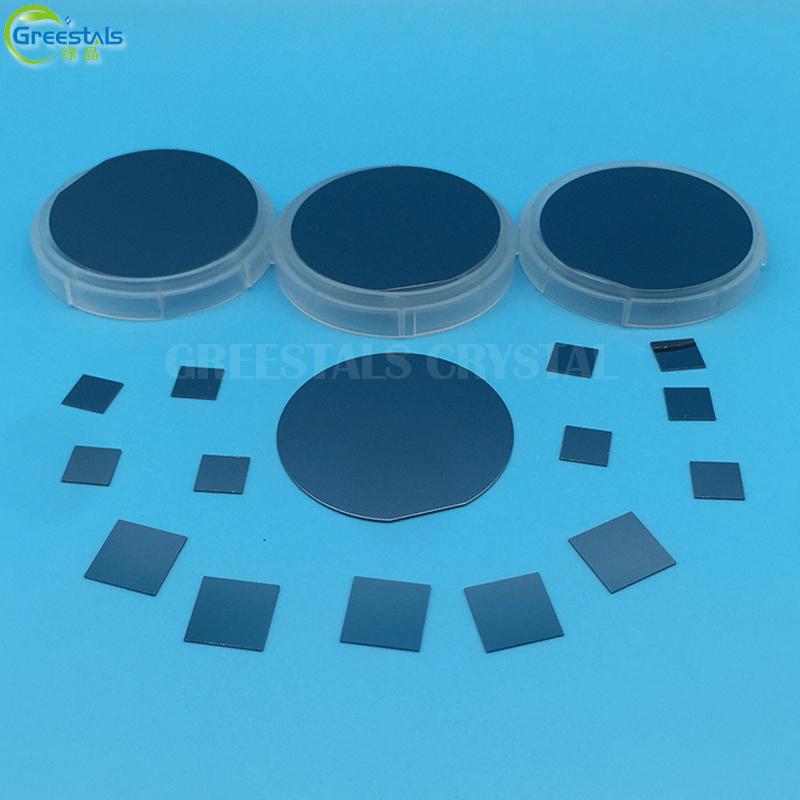
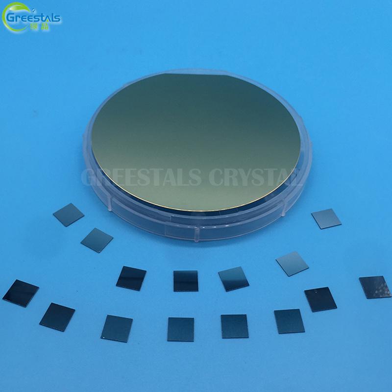
100 clean bag,1000 exactly clean bagProduct Detail
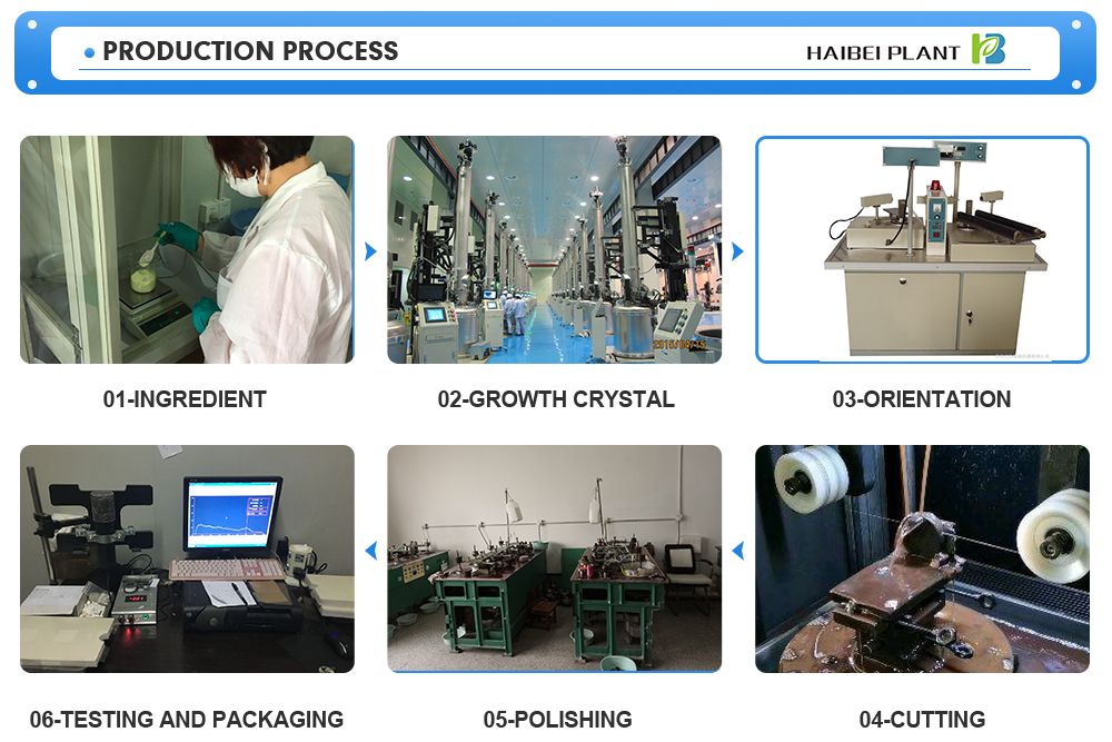
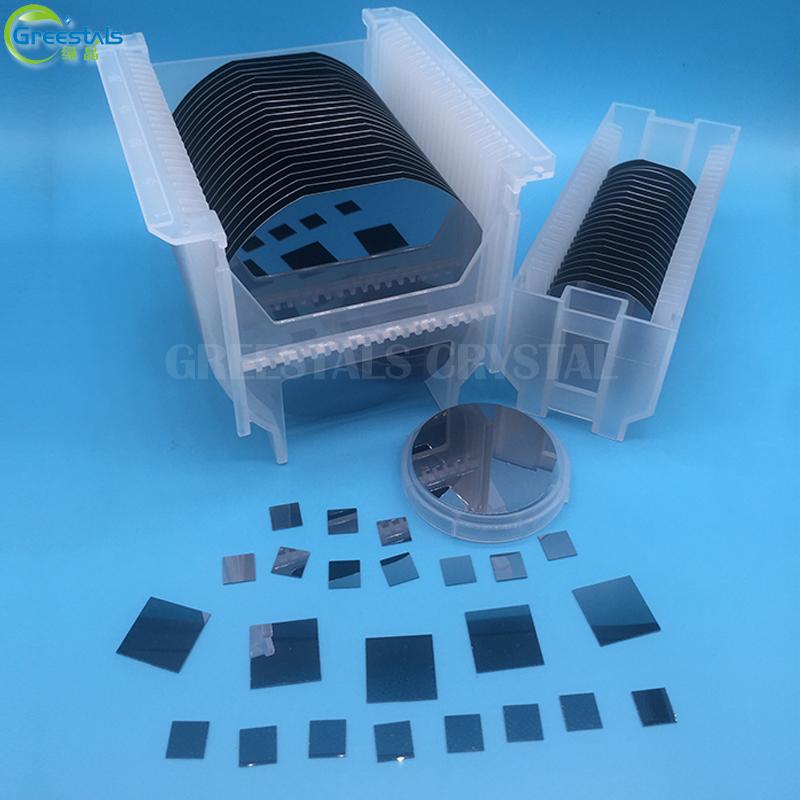
Process flow
Packaging
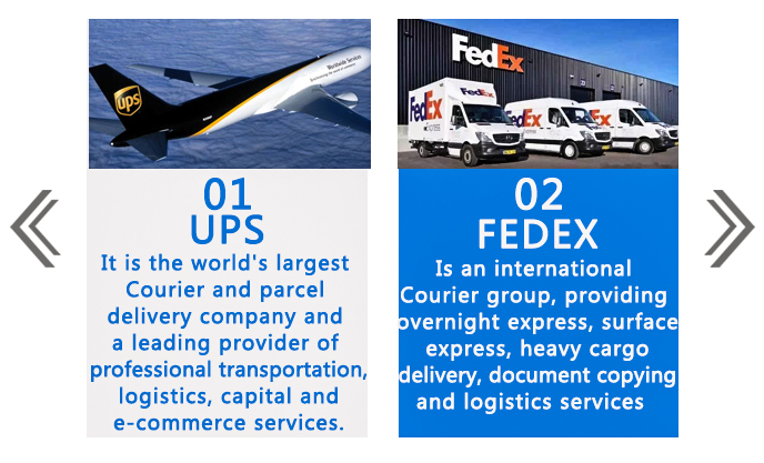
Transportation
FAQ
GaSb single crystal substrate
GaSb single crystals match the lattice constants of various ternary and quaternary, III-V compound solid solutions with bands in the 0.8~4.3um wide spectral range because of its lattice constant , because GaSb can be used as a substrate material Used to prepare lasers and detectors suitable for certain infrared optical fiber transmission, GaSb is also predicted to have a lattice-limited mobility greater than GaAs , making it a potential application prospect in the manufacture of microwave devices. The main growth methods of GaS single crystal materials include traditional liquid-sealed Czochralski technology ( LEC ), improved LEC technology, moving heating method / vertical gradient solidification technology ( VGF ) / vertical Bridgman
|
Crystals
|
Structure
|
Crystal orientation
|
Melting point
o C
|
Density
g/cm 3
|
Forbidden band width
|
|
|
GaSb
|
Cubic
a=6.094A
|
<100>
|
712
|
5.53
|
0.67
|
|
|
Main performance parameters
|
|||||||
|
Single crystal
|
Doping
|
Conductivity type
|
Carrier concentration
cm -3
|
Mobility (cm 2 /Vs)
|
Dislocation density (cm -2 )
|
Standard substrate
|
|
|
GaSb
|
Intrinsic
|
P
|
(1-2)*10 17
|
600-700
|
《1*10 4
|
Φ2″×0.5mm
Φ3″×0.5mm
|
|
|
GaSb
|
Zn
|
P
|
(5-100)*10 17
|
200-500
|
《1*10 4
|
Φ2″×0.5mm
Φ3″×0.5mm
|
|
|
GaSb
|
Te
|
N
|
(1-20) ´ 10 17
|
2000-3500
|
《1*10 4
|
Φ2″×0.5mm
Φ3″×0.5mm
|
|
|
Size (mm)
|
Dia50.8x0.5mm, 10×10×0.5mm, 10×5×0.5mm can be customized according to customer needs, special orientation and size of the substrate
|
||||||
|
Surface roughness
|
Surface roughness(Ra):<=5A
Atomic particle microscopy (AFM) test report can be provided |
||||||
|
polishing
|
Single-sided or double-sided
|
||||||
|
Packing
|
Class 100 clean bag, Class 1000 super clean room
|
||||||


711, Block B, Greenland Blue Sea, Government District, Hefei, Anhui, China
Tel : 0086-13721114787
Whatsapp : 13721114787
Email : info@haibeiflavor.com


Friendly Links :