
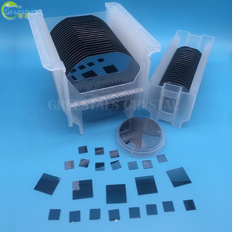
Item NO.:
GS-C012Payment:
L/C、 Western Union、 D/P、 T/TProduct Origin:
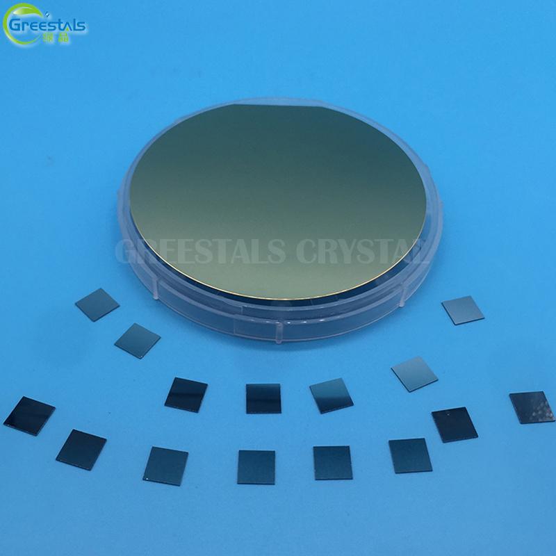
Anhui, ChinaMax Size:
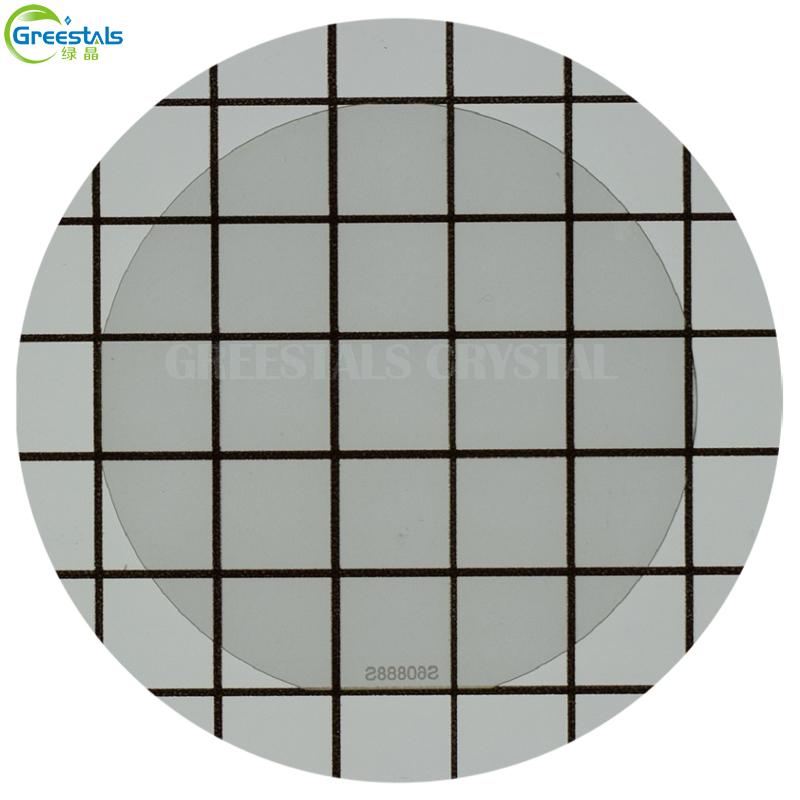
Dia100mmOrientation:
<0001>、<10-10>Package:
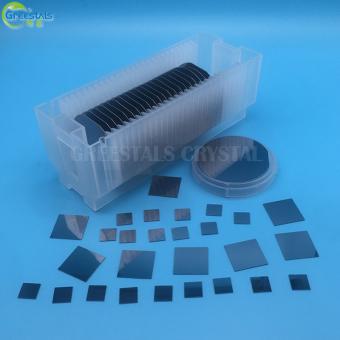
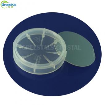
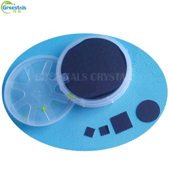
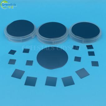
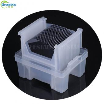
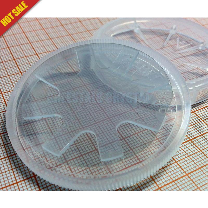
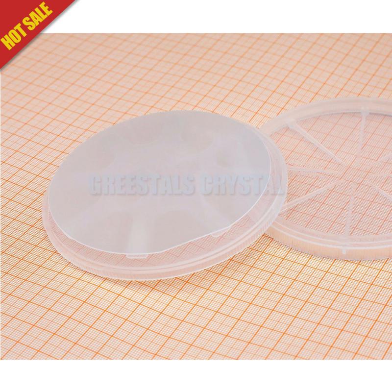
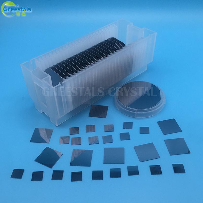
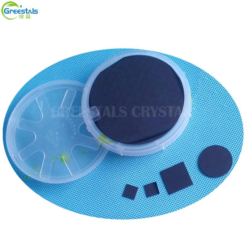
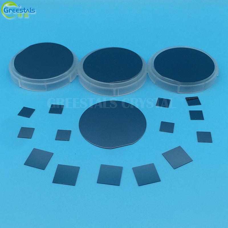
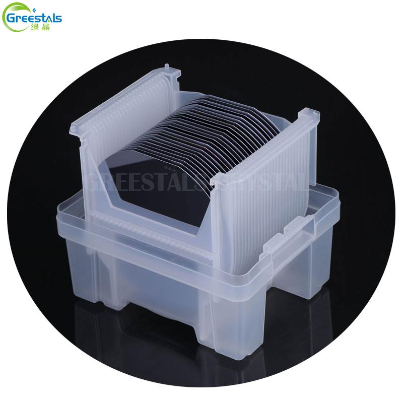
100 clean bag,1000 exactly clean bagProduct Detail
Specification
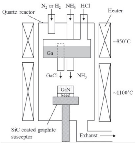
Process flow
Packaging
Transportation
FAQ
2 Inch Free-standing GaN Wafer Specification
|
Item |
Specification |
|||
|
crystalspecification |
Production(Pgrade) |
Research(Rgrade) |
Dummy(Dgrade) |
|
|
Crystaltype |
Singlecrystal |
|||
|
Orientation |
(0 0 0 1) Gaface |
|||
|
C-plane off angle towardM-axis |
0.5° ±0.15° |
|||
|
C-plane off angle towardA-axis |
0° ±0.15° |
|||
|
(002)FWHM |
< 100 arcsec |
|||
|
(102)FWHM |
< 100 arcsec |
|||
|
Latticeradiusofcurvature |
> 10 m (measured at 80% xdiameter) |
|||
|
Electricalspecification |
Dopingelements |
Room temperature resistivity(300K) |
||
|
N-type(Silicon) |
≤0.02ohm-cm |
|||
|
UID |
≤0.2ohm-cm |
|||
|
Semi-Insulating(Carbon) |
> 1E8ohm-cm |
|||
|
Shapespecification |
||||
|
Majorflatorientation |
M-plane (10-10), ±2°(st),±2° ( |
|||


711, Block B, Greenland Blue Sea, Government District, Hefei, Anhui, China
Tel : 0086-13721114787
Whatsapp : 13721114787
Email : info@haibeiflavor.com


Friendly Links :