Item NO.:
GS-C024Payment:
L/C、 Western Union、 D/P、 T/TProduct Origin:
Anhui, ChinaMax Size:
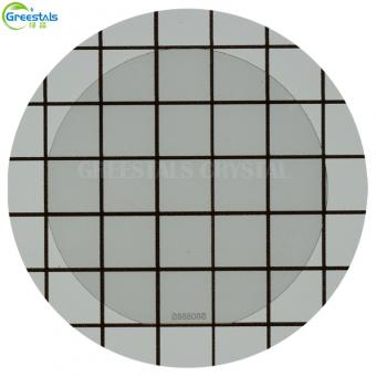
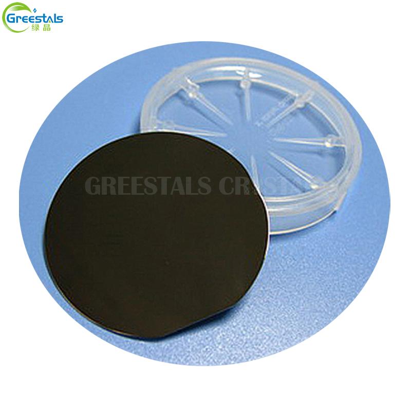
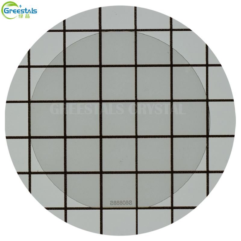
Dia76.5mmOrientation:
<100>、<110>、<111>Package:
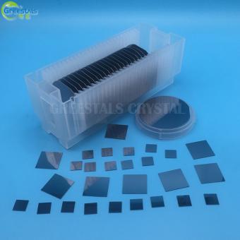
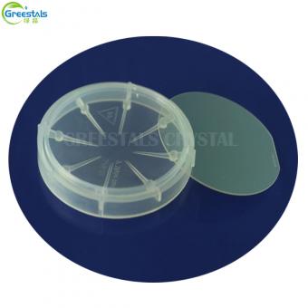
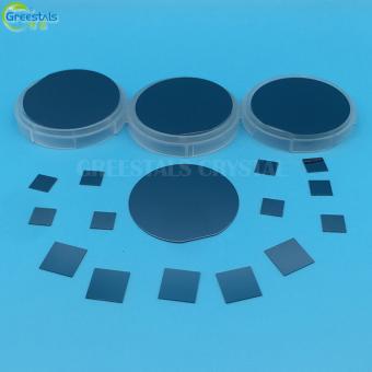
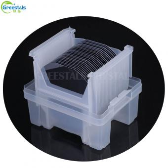
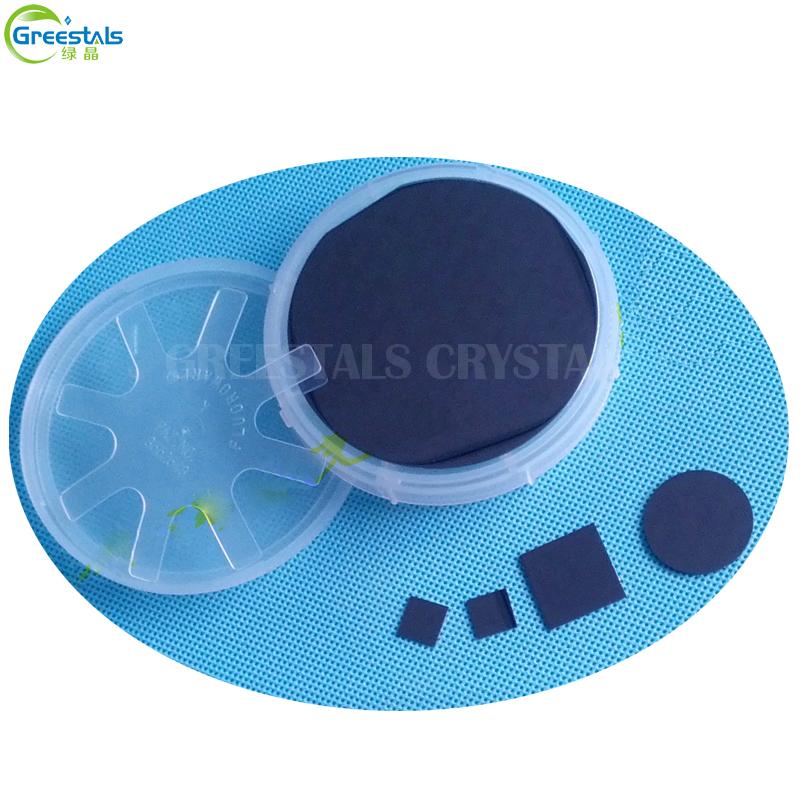
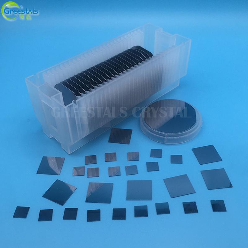
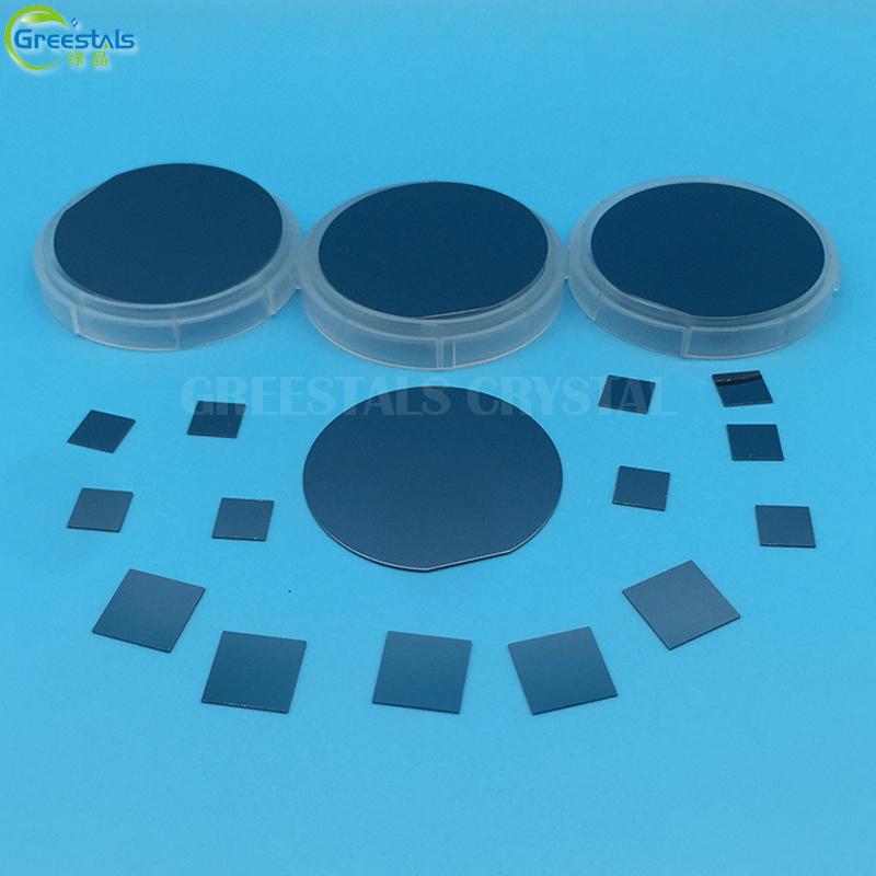
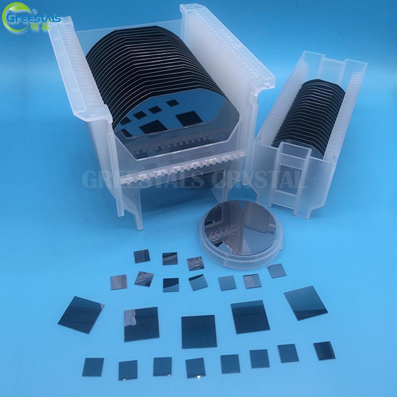
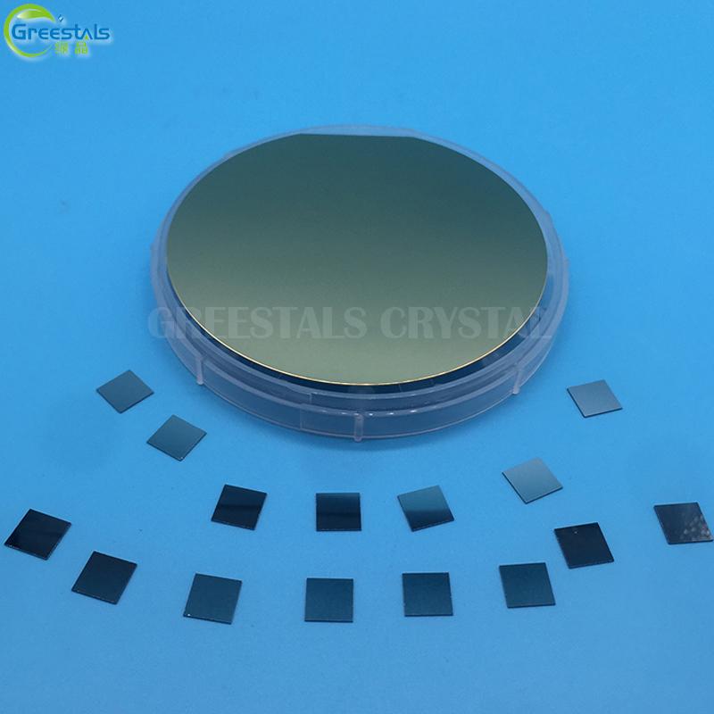
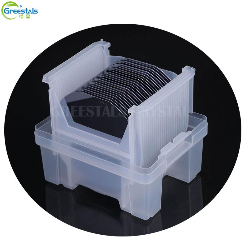
100 clean bag,1000 exactly clean bagProduct Detail
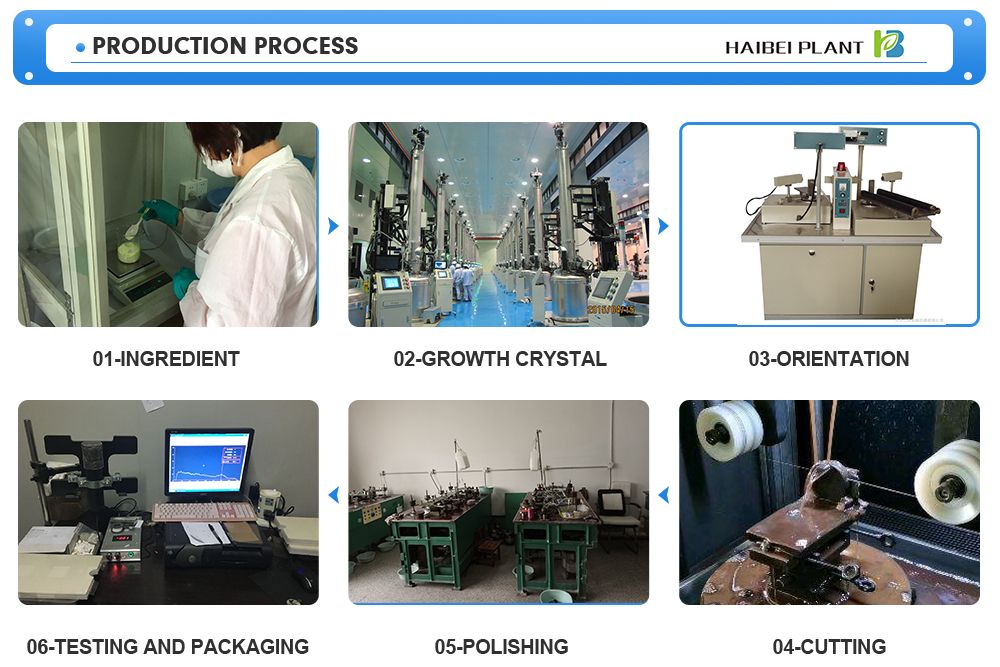
Process flow
Packaging
Transportation
FAQ
InAs single crystal substrate
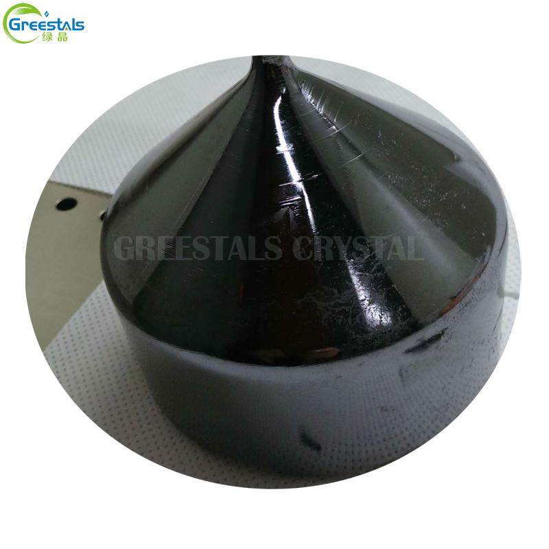
In InAs single crystal substrate can be grown as the InAsSb / the In - AsPSb, InNAsSb other heterostructure , that a wavelength 2 ~ 14 [mu] m infrared light emitting device, with InAs single crystal substrate also can be epitaxially grown AlGaSb superlattice structure materials , Production of mid-infrared quantum cascade lasers. . The infrared devices have a good prospect in the field of gas monitoring, and other low-loss optical fiber communication . Further , InAs single crystal having a high electron mobility , is making a Hall over the material of the device. As a single crystal substrate , InAs materials need to have low dislocation density, good lattice integrity, suitable electrical parameters and high uniformity . The main growth method of InP single crystal materials is the traditional liquid-sealed Czochralski technology ( LEC ).
|
Crystals
|
structure
|
Crystal orientation
|
Melting point
o C
|
density
g/cm 3
|
Forbidden band width
|
|
|
InAs
|
cube,
a=6.058 A
|
<100>
|
942
|
5.66
|
0.45
|
|
|
Main performance parameters
|
|||||||
|
Single crystal
|
Doping
|
Conductivity type
|
Carrier concentration
cm -3
|
Mobility (cm 2 /Vs)
|
Dislocation density (cm -2 )
|
Standard substrate
|
|
|
InAs
|
Intrinsic
|
N
|
5*10 16
|
2*10 4
|
<5*10 4
|
Φ2″×0.5mm
Φ3″×0.5mm
|
|
|
InAs
|
Sn
|
N
|
(5-20)*10 17
|
>2000
|
<5*10 4
|
Φ2″×0.5mm
Φ3″×0.5mm
|
|
|
InAs
|
Zn
|
P
|
(1-20) *10 17
|
100-300
|
<5*10 4
|
Φ2″×0.5mm
Φ3″×0.5mm
|
|
|
InAs
|
S
|
N
|
(1-10)*10 17
|
>2000
|
<5*10 4
|
Φ2″×0.5mm
Φ3″×0.5mm
|
|
|
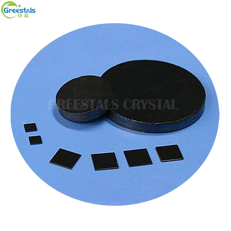
Size (mm)
|
Dia50.8x0.5mm, 10×10×0.5mm, 10×5×0.5mm can be customized according to customer needs, special orientation and size of the substrate
|
||||||
|
Surface roughness
|
Surface roughness(Ra):<=5A
Atomic particle microscopy (AFM) test report can be provided |
||||||
|
polishing
|
Single-sided or double-sided
|
||||||
|
Package
|
Class 100 clean bag, Class 1000 super clean room
|
||||||


711, Block B, Greenland Blue Sea, Government District, Hefei, Anhui, China
Tel : 0086-13721114787
Whatsapp : 13721114787
Email : info@haibeiflavor.com


Friendly Links :