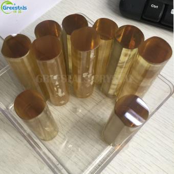
Item NO.:
GS-C046Payment:
L/C、 Western Union、 D/P、 T/TProduct Origin:
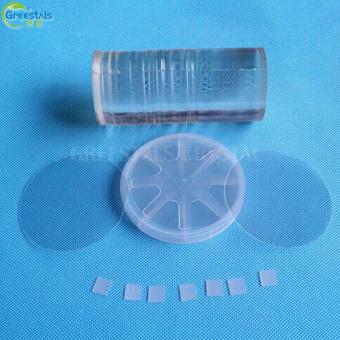
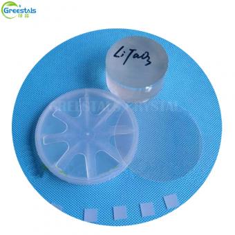
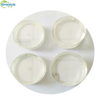
Anhui, ChinaMax Size:
dia100mmOrientation:
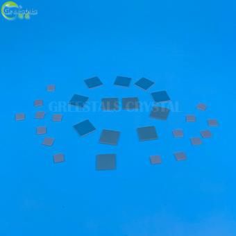
Package:
100 clean bag,1000 exactly clean bagProduct Detail
Specification
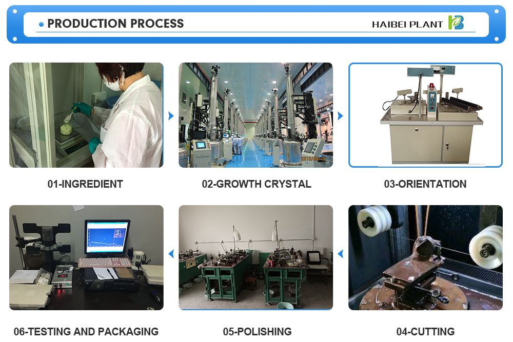
Process flow
Packaging
Transportation
FAQ
|
Main performance parameters
|
|
|
Growth method
|
Hydrothermal
|
|
Crystal structure
|
Six parties
|
|
Lattice constant
|
a=4.914Å c=5.405 Å
|
|
Melting point (℃)
|
1610°C (phase transition point: 573.1°C)
|
|
density
|
2.684g/cm 3
|
|
hardness
|
7 (mohs)
|
|
Hot Melt
|
0.18cal/gm
|
|
Thermal conductivity
|
0.0033cal/cm℃
|
|
Thermoelectric constant
|
1200uv/℃ (300℃)
|
|
Refractive index
|
1.544
|
|
Thermal expansion coefficient
|
α11: 13.71×10 6 /℃ α33: 7.48×10 6 /℃
|
|
Q value
|
1.8×10 6 min
|
|
Sound speed, sound meter level
|
3160 (m/sec)
|
|
Frequency constant
|
1661 (kHz/mm)
|
|
Piezoelectric coupling
|
K2(%) BAW: 0.65 SAW: 0.14
|
|
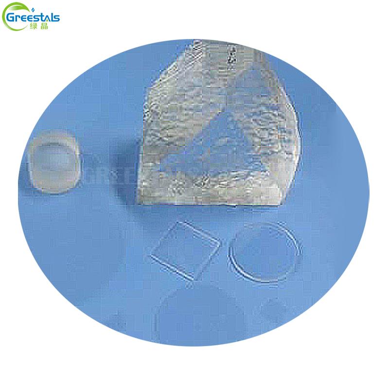
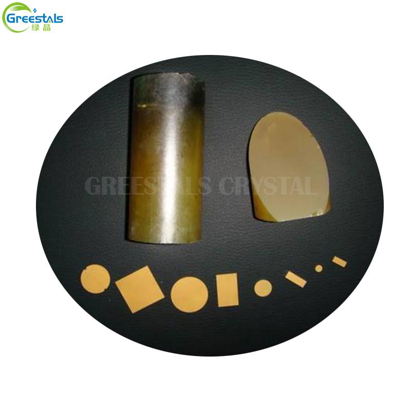
Crystal orientation
|
Y, X, or Z-cut, rotation of an arbitrary value within 30º ~ 42.75 º ± 5 minutes scope
primary orientation: according to customer requirements direction ± 30 min -time positioning side: according to customer requirements direction seed: in the center, the width <5mm , Height>66mm |
|
Polished surface
|
Epitaxial polishing: single polishing or double polishing Ra<10Å
working area: substrate diameter -3mm curvature: Φ3″<20um, Φ4″<30um working area without chipping, on the edge, chipping width <0.5mm pits and scratches :Each piece<3, every 100 pieces<20 |
|
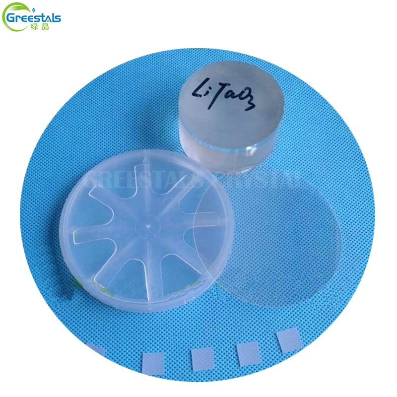
Standard thickness
|
0.5mm±0.05mm TTV<5um
|
|
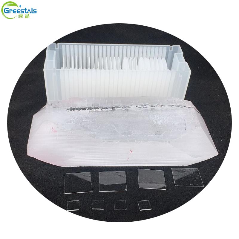
Standard diameter
|
Φ2″(50.8mm), Φ3″(76.2mm), Φ4″(100mm)±0.2mm
Primary positioning edge: 22±1.5mm (Φ3″) 32±3.0 (Φ4″) Secondary positioning edge: 10mm±1.5mm |


711, Block B, Greenland Blue Sea, Government District, Hefei, Anhui, China
Tel : 0086-13721114787
Whatsapp : 13721114787
Email : info@haibeiflavor.com


Friendly Links :